- 您现在的位置:买卖IC网 > Sheet目录1998 > ICS84314AY-02LFT (IDT, Integrated Device Technology Inc)IC SYNTHESIZER 700MHZ 32-LQFP
ICS84314-02
700MHZ, CRYSTAL-TO-3.3V/2.5V LVPECL FREQUENCY SYNTHESIZER W/FANOUT BUFFER
IDT / ICS 3.3V/2.5V LVPECL FREQUENCY SYNTHESIZER
16
ICS84314AY-02 REV. A MARCH 24, 2009
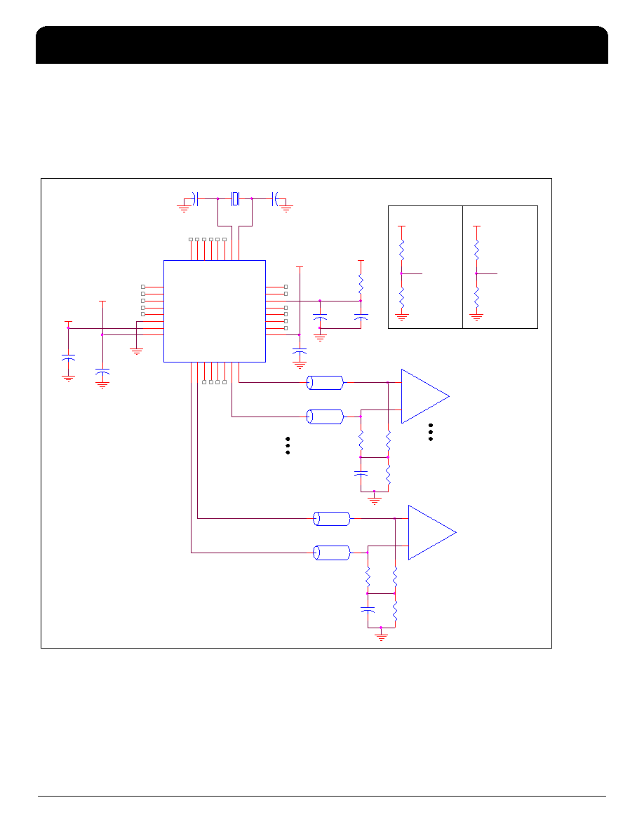
Layout Guideline
The schematic of the ICS84314-02 layout example used in this
layout guideline is shown in Figure 8A. The ICS84314-02
recommended PCB board layout for this example is shown in
Figure 8B. This layout example is used as a general guideline. The
layout in the actual system will depend on the selected component
types, the density of the components, the density of the traces, and
the stack up of the P.C. board.
Figure 8A. ICS84314-02 Schematic of Recommended Layout
C5
0.1u
VCCO=3.3V
VCC
R2
50
X1
Set Logic
Input to
'1'
RU2
Not Install
C4
0.1u
Zo = 50 Ohm
VCC
C3
0.1u
R7
10
R5
50
Set Logic
Input to
'0'
VC
C
C7 (Option)
0.1u
To Logic
Input
pins
R3
50
RU1
1K
Logic Input Pin Examples
+
-
VCC
VCCA
U1
ICS84314_02
1
2
3
4
5
6
7
8
9 10 11 12 13 14 15 16
17
18
19
20
21
22
23
24
32 31 30 29 28 27 26 25
M4
M5
M6
M7
M8
VEE
VCC
VCCO
Q0 nQ0 Q1 nQ1 Q2 nQ2 Q3 nQ3
VCCO
MR
S_CLOCK
S_DATA
S_LOAD
VCCA
XTAL_SEL
T_CLK
M3 M2 M1 M0
V
C
O
_SEL
nP_LO
AD
X_O
U
T
X_I
N
C1
RD1
Not Install
C2
Zo = 50 Ohm
VCC
VCC=3.3V
VCCO
RD2
1K
Zo = 50 Ohm
C6 (Option)
0.1u
VCCO
C11
0.01u
C16
10u
R4
50
R1
50
R6
50
To Logic
Input
pins
+
-
发布紧急采购,3分钟左右您将得到回复。
相关PDF资料
ICS843156AKILF
IC CLK GENERATOR 32VFQFP
ICS843156AKLF
IC CLK GENERATOR 32VFQFP
ICS843202AYILF
IC SYNTHESIZER 680MHZ 32-LQFP
ICS843204AGILF
IC SYNTHESIZER LVPECL 48-TSSOP
ICS84320AY-01LN
IC SYNTHESIZER GP LVPECL 32-LQFP
ICS84320AYI-01LF
IC FREQ SYNTHESIZER 32TQFP
ICS843251AG-04LF
IC CLK GENERATOR LVPECL 8-TSSOP
ICS843251AGI-14LF
IC CLK GEN ETHERNET 25MHZ 8TSSOP
相关代理商/技术参数
ICS84314AY-02T
制造商:ICS 制造商全称:ICS 功能描述:700MHZ, CRYSTAL-TO-3.3V/2.5V LVPECL FREQUENCY SYNTHESIZER W/FANOUT BUFFER
ICS84314AYLF
功能描述:IC SYNTHESIZER 350MHZ 32-LQFP RoHS:是 类别:集成电路 (IC) >> 时钟/计时 - 时钟发生器,PLL,频率合成器 系列:HiPerClockS™ 标准包装:1,000 系列:- 类型:时钟/频率合成器,扇出分配 PLL:- 输入:- 输出:- 电路数:- 比率 - 输入:输出:- 差分 - 输入:输出:- 频率 - 最大:- 除法器/乘法器:- 电源电压:- 工作温度:- 安装类型:表面贴装 封装/外壳:56-VFQFN 裸露焊盘 供应商设备封装:56-VFQFP-EP(8x8) 包装:带卷 (TR) 其它名称:844S012AKI-01LFT
ICS84314AYLFT
功能描述:IC SYNTHESIZER 350MHZ 32-LQFP RoHS:是 类别:集成电路 (IC) >> 时钟/计时 - 时钟发生器,PLL,频率合成器 系列:HiPerClockS™ 标准包装:1,000 系列:- 类型:时钟/频率合成器,扇出分配 PLL:- 输入:- 输出:- 电路数:- 比率 - 输入:输出:- 差分 - 输入:输出:- 频率 - 最大:- 除法器/乘法器:- 电源电压:- 工作温度:- 安装类型:表面贴装 封装/外壳:56-VFQFN 裸露焊盘 供应商设备封装:56-VFQFP-EP(8x8) 包装:带卷 (TR) 其它名称:844S012AKI-01LFT
ICS84314AYT
制造商:ICS 制造商全称:ICS 功能描述:350MHZ, CRYSTAL-TO-3.3V/2.5V LVPECL FREQUENCY SYNTHESIZER W/FANOUT BUFFER
ICS843156AKILF
功能描述:IC CLK GENERATOR 32VFQFP RoHS:是 类别:集成电路 (IC) >> 时钟/计时 - 时钟发生器,PLL,频率合成器 系列:HiPerClockS™ 标准包装:1,000 系列:- 类型:时钟/频率合成器,扇出分配 PLL:- 输入:- 输出:- 电路数:- 比率 - 输入:输出:- 差分 - 输入:输出:- 频率 - 最大:- 除法器/乘法器:- 电源电压:- 工作温度:- 安装类型:表面贴装 封装/外壳:56-VFQFN 裸露焊盘 供应商设备封装:56-VFQFP-EP(8x8) 包装:带卷 (TR) 其它名称:844S012AKI-01LFT
ICS843156AKILFT
功能描述:IC CLK GENERATOR 32VFQFP RoHS:是 类别:集成电路 (IC) >> 时钟/计时 - 时钟发生器,PLL,频率合成器 系列:HiPerClockS™ 标准包装:1,000 系列:- 类型:时钟/频率合成器,扇出分配 PLL:- 输入:- 输出:- 电路数:- 比率 - 输入:输出:- 差分 - 输入:输出:- 频率 - 最大:- 除法器/乘法器:- 电源电压:- 工作温度:- 安装类型:表面贴装 封装/外壳:56-VFQFN 裸露焊盘 供应商设备封装:56-VFQFP-EP(8x8) 包装:带卷 (TR) 其它名称:844S012AKI-01LFT
ICS843156AKLF
功能描述:IC CLK GENERATOR 32VFQFP RoHS:是 类别:集成电路 (IC) >> 时钟/计时 - 时钟发生器,PLL,频率合成器 系列:HiPerClockS™ 标准包装:1,000 系列:- 类型:时钟/频率合成器,扇出分配 PLL:- 输入:- 输出:- 电路数:- 比率 - 输入:输出:- 差分 - 输入:输出:- 频率 - 最大:- 除法器/乘法器:- 电源电压:- 工作温度:- 安装类型:表面贴装 封装/外壳:56-VFQFN 裸露焊盘 供应商设备封装:56-VFQFP-EP(8x8) 包装:带卷 (TR) 其它名称:844S012AKI-01LFT
ICS843156AKLFT
功能描述:IC CLK GENERATOR 32VFQFP RoHS:是 类别:集成电路 (IC) >> 时钟/计时 - 时钟发生器,PLL,频率合成器 系列:HiPerClockS™ 标准包装:1,000 系列:- 类型:时钟/频率合成器,扇出分配 PLL:- 输入:- 输出:- 电路数:- 比率 - 输入:输出:- 差分 - 输入:输出:- 频率 - 最大:- 除法器/乘法器:- 电源电压:- 工作温度:- 安装类型:表面贴装 封装/外壳:56-VFQFN 裸露焊盘 供应商设备封装:56-VFQFP-EP(8x8) 包装:带卷 (TR) 其它名称:844S012AKI-01LFT